

No products.
No products.
|
Intelligent anti stupidity and anti re carving |
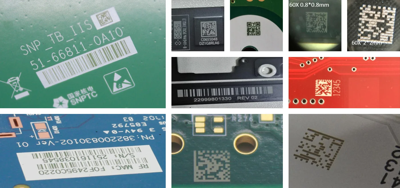
Industry minimum laser spot diameter 0.11mm |
|
Laser stability: fluctuation rate of output power |
Customized MES system docking |
|
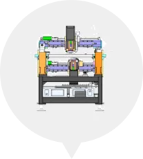
Upper and lower head / three section varus unit |
Self test reading rate: 100% |
|
Laser imported from the United States |
High-precision visual navigation system |
|
Light-weight design laser module |
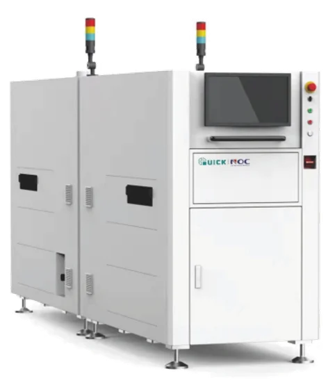
Providing high-precision laser marking, coding, and surface-processing solutions designed for electronics manufacturing, SMT components, industrial products, and applications requiring absolute traceability. The systems are engineered for smart operation, long-term stability, and maximum automation, helping increase productivity, reduce human error, and ensure uniform marking quality on all materials.
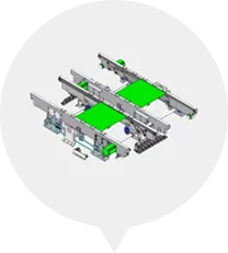
👉 Direct mount double track
👉 Independent engraving mode
👉 Independent transmission plate
👉 A side and B side are engraved at the same time
👉 100% increase in efficiency
👉 Double side code printing, front and back flip
👉 Reduce transmission time and improve efficiency by 30%
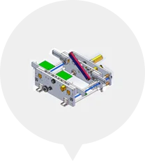
👉 Step by step programming step
👉 One click point selection design
👉 Multi module custom barcode editing rules
Operating process
1. Loading machine feeding
2. Feeding into receiving track
3. CCDpositioning / code reading
4. Magnetic levitation platform positioning
5. Transfer the carrier board to the marking position
6. Automated laser marking
7. Base plate cleaning
8. Feeding into receiving track
9. CCD detection and identification
10. Receiving operation of receiving machine
No account yet?
Create an Account
